
Stencil Printing in Micro Via
Stencil printing is a very common technique in the manufacture of many different products including home decor, arts and crafts, and manufacturing. You can find stencils that are made from a variety of materials including mylar, PETG and a range of different plastics. It is important to remember that stencils must be treated carefully and used with care to ensure the best results. When using a stencil it is important to use a clean screen and to remove any excess ink from the stencil before washing it. This will help to prevent the etching of the stencil and will allow for a longer life.
The printed circuit board (PCB) assembly process is a critical part of the production of electronic micro via. It consists of three sub-processes: solder paste stencil printing application, component placement, and solder reflow to form strong metal solder joints between the PCB and surface mount devices. Changing consumer demand for more efficient and smaller electronics has resulted in the continued trend towards miniaturization of surface mount components. This has led to increased demands on the surface mount technology (SMA) process, particularly solder paste stencil printing application.
On average, 60% of end-of-line soldering defects can be attributed to poor stencil printing performance. As a result, solder paste stencil printing is a very challenging quality assurance process.
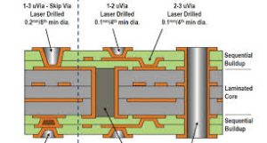
The Role of Stencil Printing in Micro Via
Stencil design, material and blade selection are key to successful stencil printing. Aspect ratio (aperture width divided by stencil foil thickness) is a very important design parameter, as it determines the potential volume of solder paste applied to the PCB or substrate. Squeegee blades come in two different types – metal and polyurethane, with metal squeegees being the preferred choice as they are better resistant to scooping paste from the stencil aperture walls when printing.
In the early days of laser-cut stencils, etching would occur both vertically and laterally, causing extra solder deposit. This was overcome by the development of hybrid stencils where large apertures are Chemically Etched while small apertures are laser-cut. In addition, a new generation of stencil material has emerged, known as conductive foam (CF) that is not affected by undercutting and can be cut very accurately with lasers.
Blind, buried and micro vias are essential tools in the arsenal of the modern PCB designer. They enable designers to route signals and power through multiple layers, thereby minimizing the overall board thickness while still meeting minimum trace width requirements.
To maximize the benefit of these specialized features, designers should be aware of their limitations and consider the implications when designing a PCB. For example, stacked microvias may require additional copper layers that can increase the risk of shorting between a metallurgical junction and a neighboring via or pad. This is why a good understanding of the capabilities and limitations of stacked microvias is crucial to achieving high-performance electronic products. In addition, a comprehensive test plan should be in place to identify the critical failure points and correct them with appropriate design changes.