
RF PCBs ensure signal isolation
In the realm of high-frequency circuit design, especially in RF (Radio Frequency) systems, signal isolation is critical to ensure that signals remain intact and interference is minimized. RF PCBs (Printed Circuit Boards) play a crucial role in maintaining the integrity of signals by ensuring that unwanted coupling or interference between different signal paths is prevented. This isolation is essential for achieving high-performance systems in applications such as telecommunications, satellite communication, radar, and wireless networking. RF PCBs utilize a combination of design techniques, materials, and layout strategies to ensure signal isolation and optimize overall system performance.
One of the primary methods by which RF PCBs ensure signal isolation is through careful layout and trace routing. In high-frequency designs, signals are transmitted along traces on the PCB, and improper routing can lead to unintended coupling between traces, resulting in cross-talk or signal interference. To mitigate this, RF designers use techniques such as physical separation between signal paths. By ensuring that signal traces are adequately spaced, RF PCBs reduce the likelihood of coupling between them. Additionally, traces that carry high-frequency or sensitive signals are often routed away from other high-power or noisy traces to avoid interference. A good PCB layout also minimizes the use of vias, which can add inductance and introduce unwanted coupling, helping to preserve signal isolation.
Another key design strategy employed in rf pcb is the use of ground planes. A solid, continuous ground plane acts as a shield to help isolate signals from each other and from external sources of interference. The ground plane provides a low-resistance return path for the signals and serves as a reference point for the entire PCB. By routing traces over the ground plane and ensuring a solid connection between the ground and the PCB components, designers can significantly reduce the chances of signal interference. The ground plane also helps to limit the path for electromagnetic radiation, ensuring that signals do not radiate unwanted energy into other parts of the circuit or external environments. This effective grounding is crucial for maintaining high signal integrity and ensuring minimal interference between different signal paths.
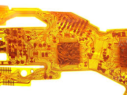
How do RF PCBs ensure signal isolation?
To further improve signal isolation, shielding is often incorporated into the PCB design. Shielding involves creating a physical barrier around sensitive areas of the PCB or around individual components that might be prone to interference. This is typically done using metal cans or enclosures that isolate specific sections of the PCB from external electromagnetic interference (EMI) or signals from other parts of the circuit. In addition to shielding components, RF PCBs may also use closed-loop shielding to surround entire signal paths or power delivery areas, preventing external signals from coupling into sensitive traces. By reducing the impact of EMI, shielding enhances signal isolation and overall system performance.
Another important factor in ensuring signal isolation is impedance matching. When the impedance of different sections of the PCB is mismatched, signals can reflect, leading to loss of signal strength or even cross-talk between traces. RF designers carefully match the impedance of traces, connectors, and components to avoid such issues. By ensuring consistent impedance throughout the PCB, signals are transmitted with minimal reflection, which directly helps maintain isolation between signal paths. The use of controlled impedance traces ensures that signals travel along their intended paths without interacting with adjacent traces or components, preserving the integrity of each signal.
In addition to these design techniques, the choice of materials used in RF PCBs is crucial for ensuring signal isolation. Substrate materials with low dielectric constants are often chosen for RF designs because they reduce signal attenuation and interference. Materials like PTFE (Polytetrafluoroethylene) and ceramic-filled composites offer low loss and high-frequency performance, making them ideal for RF PCBs. The dielectric properties of the substrate material can affect the speed and loss of the signal as it travels along the trace. Therefore, selecting materials with low loss characteristics ensures that the signal does not degrade as it passes through the PCB, thus maintaining signal isolation and quality.
Additionally, filtering is a technique used to further isolate and protect the signal paths. RF PCBs are designed with various types of filters—such as low-pass, high-pass, and band-pass filters—that help isolate specific frequency bands while blocking unwanted signals or noise. Filters help ensure that only the desired frequencies reach the receiver or the next stage of the system. These filters are integrated directly into the PCB design, enabling effective isolation of noise and interference from the signal path, leading to cleaner and more accurate signal transmission.