
Pcb Design & Assembly Materials
When it comes to pcb design & assembly, the thickness of your PCB is a crucial factor that determines how well it will perform. Thinner PCBs can break easily while thicker ones are less flexible but more durable and will handle higher current flows. However, the right thickness will depend on your application, profile and weight of components and connections.
The standard thickness of a PCB board is 1.6mm, which provides an ideal balance of mechanical strength and thinness. This thickness allows for a wide range of applications and can accommodate both small and large components without being too heavy for portable devices.
Thickness is determined by the thickness of the core and prepreg materials and the copper traces. It also depends on the thickness of other layers, such as solder mask and silkscreen. The thickness of the base material takes up the biggest partition in the final PCB thickness, but other factors play a role as well.
For instance, the thickness of the substrate influences the size of the insulating layer that separates the copper from the rest of the circuit board. This material can be made of various substances, including fiberglass weave or epoxy resin, and may vary in thickness depending on the desired functionalities.
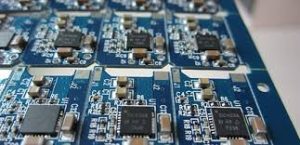
Thicknesses of Pcb Design & Assembly Materials
The choice of substrate material is influenced by the temperature tolerance of the circuit board, the conductive properties of its copper, and the dielectric constant of its insulating material. A good substrate will not only have a low glass transition temperature (Tg) and decomposition temperature (Td), but will also have low coefficient of thermal expansion. This means that it will expand at a lower rate when heated, which will minimize a change in the position of the copper traces on the circuit board.
Another important consideration when determining the thickness of your PCB is its conductor width, which defines how much current it can carry. If the current flowing through a trace is too high, it will overheat and damage the circuit board, so it is essential that you choose a conductor width that can comfortably accommodate the amount of current it will need to flow.
The copper thickness of a PCB is usually measured in ounces, and the thickness of the foil used to make up this layer is then determined by spreading an ounce of the specific copper weight evenly over a square foot area. This results in the standard copper thickness of 1.37 mils (1.37 thousandths of an inch).
Other factors that can affect the thickness of a PCB include its design, the number of layers, and the materials used for the silkscreen and solder mask. The latter is typically white but can be printed with any color ink that you choose. Silkscreen is an important part of the design process, as it can help eliminate mistakes such as traces that touch each other and incorrectly placed drill holes. It can also be used to add visual appeal to the finished circuit board.