
PCB fabrication assembly design
A good PCB (Printed Circuit Board) fabrication assembly design is essential for creating a high-quality, reliable, and cost-effective product. Whether the PCB is intended for consumer electronics, medical devices, automotive systems, or any other application, the design plays a crucial role in determining the functionality, durability, and overall performance of the final product. Achieving an effective design involves balancing multiple factors, such as electrical performance, manufacturability, cost, and ease of assembly. A well-designed PCB fabrication assembly ensures that the board functions as intended while minimizing issues like signal interference, power loss, and mechanical stress, all while being easy to fabricate and assemble.
A good PCB design starts with a clear and optimized layout. The placement of components should be organized to ensure efficient electrical performance, with minimal signal interference and reduced noise. High-speed signals, for example, should be routed as directly as possible, with short and controlled trace lengths, to avoid signal degradation. Components should be placed logically, with related parts grouped together to minimize the length of connections between them. Proper component placement also ensures that the board is easy to assemble, reducing the chances of errors during the pcb fabrication assembly process.
For ease of assembly, designers should avoid tight component placement, as this can complicate the pick-and-place process and increase the risk of misalignment. Additionally, a well-organized design should provide enough space for soldering, whether through-hole or surface mount components, to ensure that the assembly process is efficient and error-free.
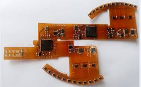
What makes a good PCB fabrication assembly design?
Designing for manufacturability (DFM) is a crucial concept in PCB fabrication assembly. This involves designing the PCB in a way that aligns with the capabilities of the manufacturing process. DFM principles help ensure that the board can be produced efficiently, with minimal defects and reduced production costs.
One key aspect of DFM is selecting the appropriate layer count for the PCB. While multi-layer designs are often necessary for complex circuits, a simpler two-layer PCB design is typically easier and cheaper to manufacture. The design should also consider the minimum trace width and spacing that the chosen fabrication process can handle. This ensures that the PCB can be reliably produced and assembled without issues related to trace width violations or unmanufacturable designs.
Signal integrity and power distribution are critical factors in PCB design, especially for high-speed or high-frequency circuits. A good design will carefully manage power delivery and ensure stable, noise-free operation. This involves careful planning of the power and ground planes to reduce impedance and minimize the chances of power loss or interference. Additionally, designers should consider the use of decoupling capacitors and proper routing of power traces to ensure the effective distribution of power across the PCB.
Signal integrity is equally important, particularly for sensitive analog circuits or high-speed digital circuits. Designers must carefully route traces to minimize signal reflection, cross-talk, and electromagnetic interference (EMI). By ensuring that the traces are kept short and impedance-controlled, the board can maintain high signal integrity, which is essential for the proper functioning of the PCB.
Thermal management is an often-overlooked aspect of PCB fabrication assembly design, but it is crucial for maintaining the reliability and performance of the board. Components generate heat during operation, and without proper heat dissipation, the PCB can suffer from thermal stress, leading to component failure or reduced lifespan. A good PCB design will incorporate heat management techniques such as adding heat sinks, using thermally conductive materials, and ensuring proper spacing between components to allow airflow.
Designers should also consider using larger copper pads and traces for power components that generate more heat, as these can act as heat sinks, helping to dissipate heat more effectively. Additionally, placing components that generate heat away from sensitive or heat-sensitive components can reduce the risk of thermal damage.
A good PCB fabrication assembly design should also be designed for easy testing and high reliability. Including test points in the design allows for easier and more thorough electrical testing during the assembly process, ensuring that the PCB works as expected before it moves on to the next phase. A reliable design also means minimizing the potential for failure during operation. This can be achieved by using high-quality components, ensuring solid solder joints, and considering the long-term performance of the PCB under varying environmental conditions.
A good PCB design is also cost-effective. Designers must balance the cost of components, materials, and manufacturing processes to ensure the PCB can be produced within the budget. Choosing standard components, optimizing the layout for efficient use of materials, and selecting an appropriate number of layers for the PCB can all help reduce costs. Additionally, the design should avoid overly complex features that add unnecessary expense without providing significant benefits to the functionality of the PCB.